200+
Full-time research staff
100+
Patents
200 Million +
Annual investment in R&D
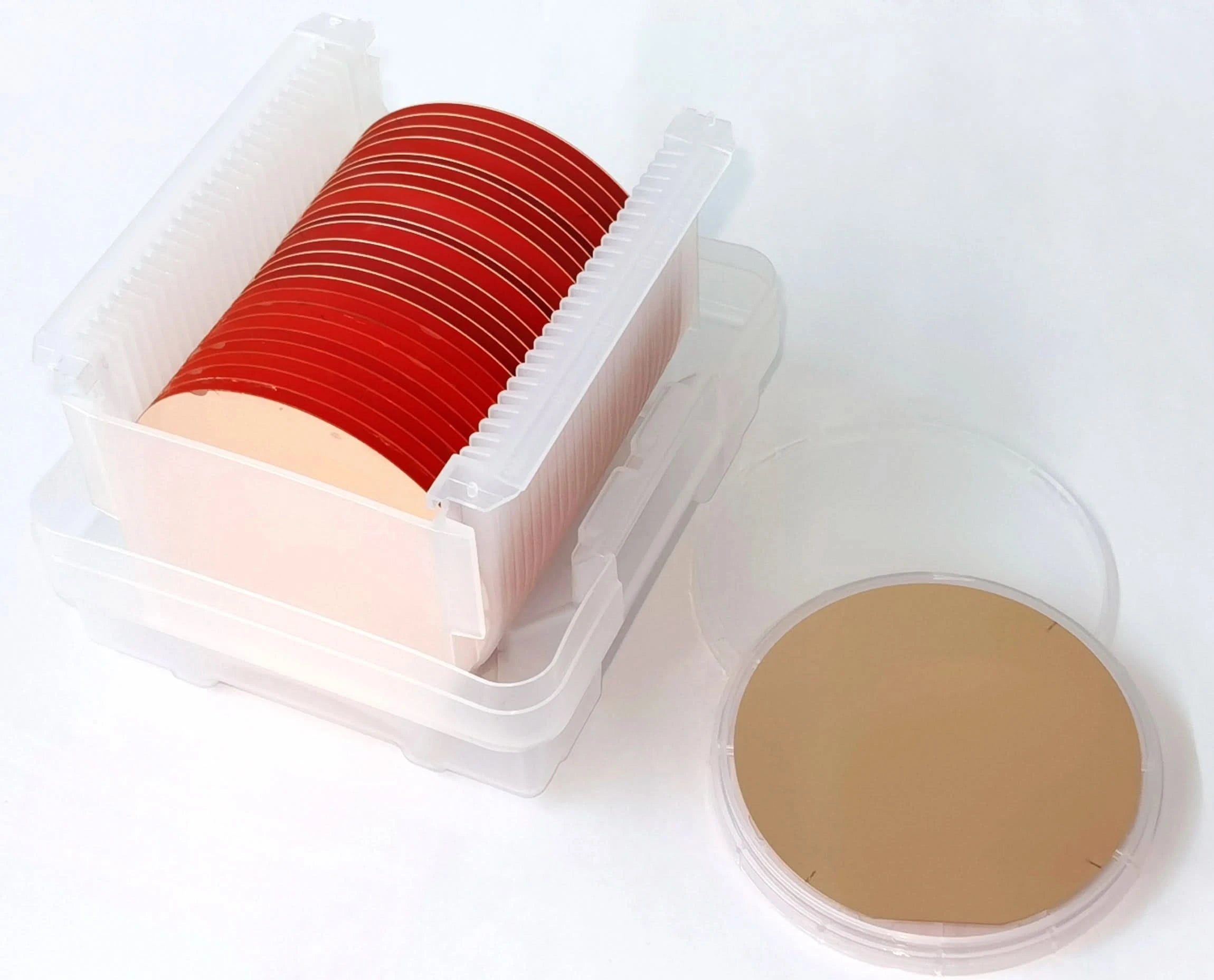
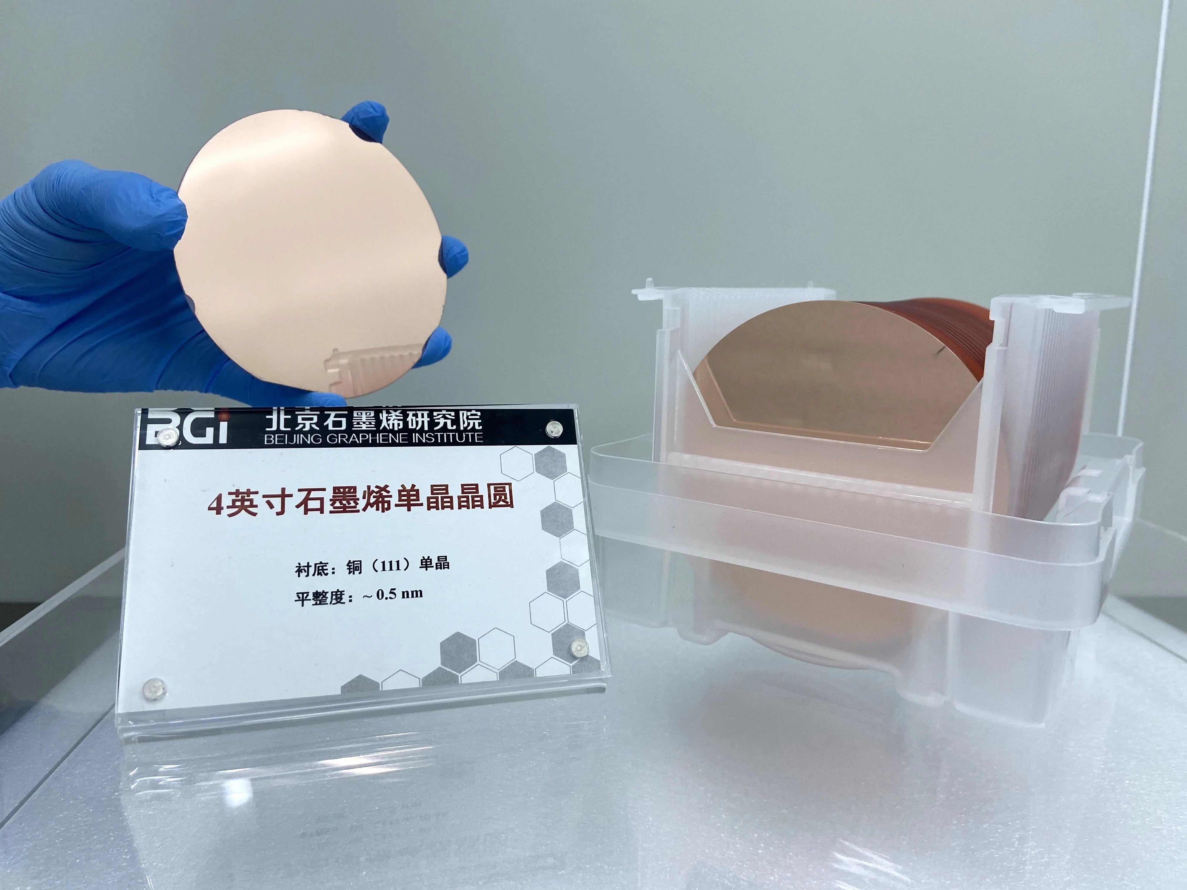
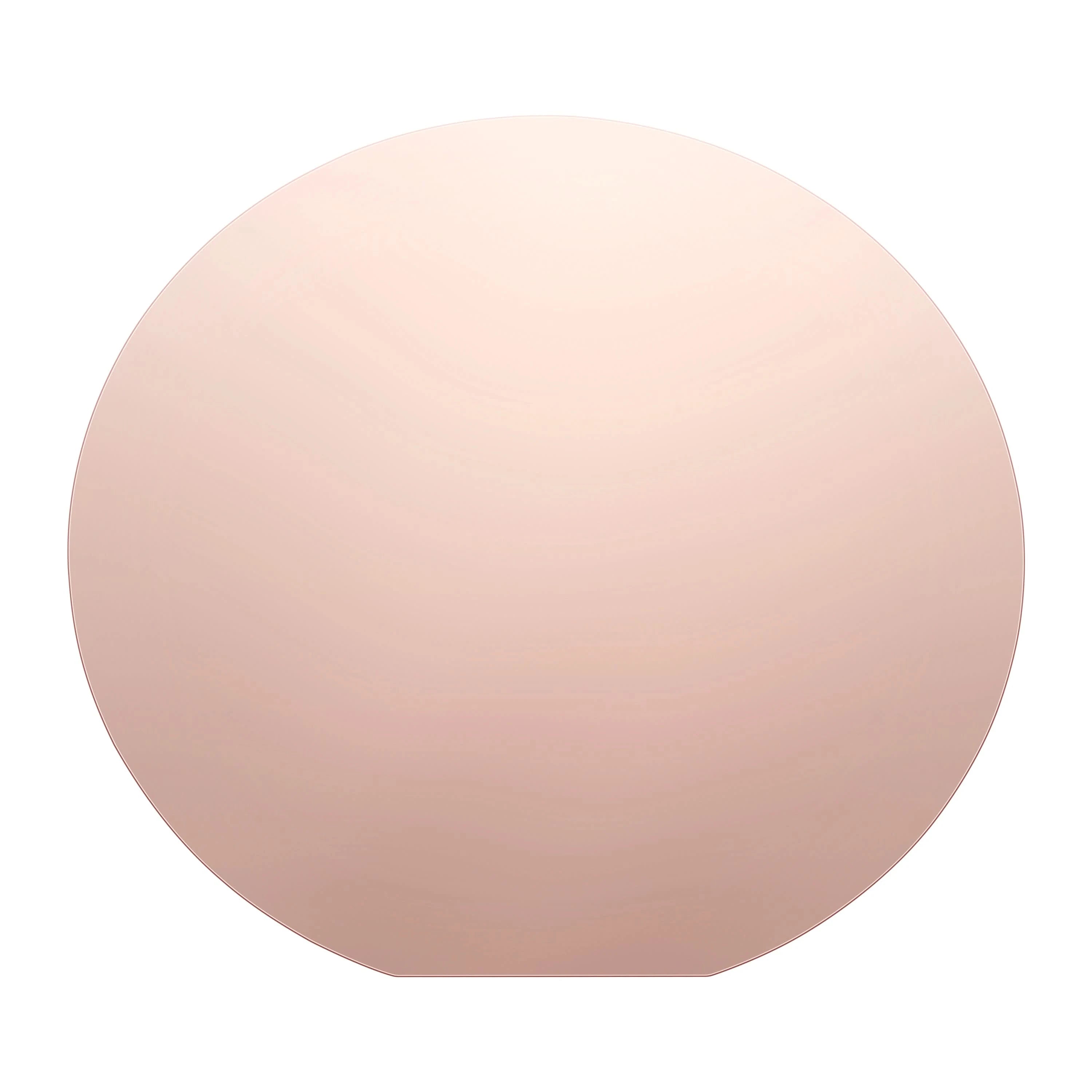

Ultra-flat, high-quality graphene with exceptional electronic properties. Perfect for semiconductor research, flexible electronics, sensors, and advanced nanotechnology applications.
The high-quality materials provided by BGI have greatly supported our research on integrated circuit systems, pushing forward our breakthroughs.

BGI's graphene wafers have played a vital role in our research on the transport mechanisms of crystal materials and optoelectronic devices.

BGI Graphene grids are probably of the best quality we have received with a beautiful single layer of graphene coating, and actually we have two protein systems that were frozen on them and behaved very nicely when looking at the particle distribution and homogeneity on a Krios.

The advanced graphene wafers from BGI have been fundamental in pushing forward our research on optoelectronic systems, contributing significantly to our progress.

FAQ
What is single-crystalline CVD Graphene?
Single-crystal CVD Graphene refers to CVD graphene films grown on single-crystal growth substrates, such as single-crystal copper wafers and single-crystal copper foils. The single-crystal copper films can either be in the form of foil or on a sapphire wafer.
Graphene has high transparency. How do you measure the coverage of graphene on copper foil?
Our researchers use optical microscopy to observe and distinguish between graphene and the copper substrate (copper foil) based on different contrast levels. Simultaneously, our researchers input the contrast data into our self-developed computer software for comprehensive analysis of the coverage rate.
What is the thickness of the single-crystal copper foil substrate?
Depending on the size, the thickness range is 28-50 μm.
What is the thickness of the copper layer on the single-crystal wafer?
500 nm


