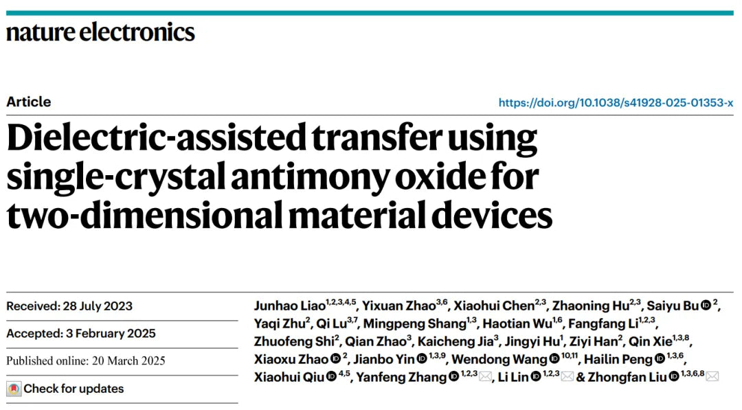
High-quality wafer-scale graphene is foundational for the development of next-generation optoelectronic devices. While large-area, wrinkle-free single-crystal graphene films have already been successfully synthesized on metal substrates, the challenge of transferring these films onto target substrates without damage—while preserving their intrinsic properties—remains a key obstacle in practical device fabrication.
Addressing this challenge, a research team led by Academician Liu Zhongfan, Prof. Zhang Yanfeng, and Prof. Lin Li from Peking University has published a landmark study in Nature Electronics. The team presents a novel approach using epitaxially grown single-crystal antimony oxide (Sb₂O₃) as a dielectric encapsulation and transfer aid to enable damage-free transfer of 4-inch graphene wafers and the fabrication of high-performance device arrays.
Why It Matters: Limitations of Traditional Transfer Methods
Conventional polymer-assisted transfer techniques often result in structural damage and surface contamination, which significantly degrade graphene’s electrical properties. Moreover, in real-world applications, encapsulation materials such as hexagonal boron nitride (h-BN) are often required to ensure the long-term stability of graphene devices.
In this study, the research team epitaxially grew high-quality Sb₂O₃ dielectric layers on Cu(111)/graphene templates, achieving lattice-matched, single-crystalline films. Graphene served as a van der Waals buffer layer, decoupling the dielectric layer from the growth substrate and enabling clean, crack-free peeling of Sb₂O₃. Sb₂O₃ in turn functions as a support and protection layer for the graphene, facilitating a clean transfer process onto Si/SiO₂ substrates.

Key Results and Device Performance
- Transfer completeness of the 4-inch graphene wafer reached 98%, with minimal surface contamination.
- Raman spectroscopy revealed a narrow 2D peak FWHM of ~23 cm⁻¹, indicating low-defect, high-quality graphene.
- Carrier mobility peaked at 29,000 cm²V⁻¹s⁻¹, with an average of around 14,000 cm²V⁻¹s⁻¹, demonstrating excellent electronic properties.
- Even after 6 months of air exposure, device performance showed less than 10% variation, highlighting the superior encapsulation capability of Sb₂O₃.
These results mark a major advance in the scalable production and stable integration of graphene into electronic devices.

Technical Innovation: Sb₂O₃-Assisted Transfer Strategy
The success of this approach lies in the synergistic interaction between the pre-formed graphene, the Sb₂O₃ dielectric film, and the van der Waals interface:
- Sb₂O₃ provides mechanical support during transfer while protecting the graphene from external contamination.
- Its excellent dielectric properties also make it suitable for use in advanced device architectures.
- The entire process avoids polymers, reducing residue and preserving the intrinsic properties of graphene.
Broader Impact and Future Applications
This work lays a robust foundation for real-world graphene electronics, where scalability, material integrity, and long-term device stability are crucial. The demonstrated strategy is particularly relevant for flexible electronics, transparent conductors, and next-generation sensors and transistors.

About the Authors and Acknowledgments
The study was conducted by a collaborative team led by Academician Liu Zhongfan, Prof. Zhang Yanfeng, and Prof. Lin Li at Peking University.
Key contributors include:
- Prof. Qiu Xiaohui (National Center for Nanoscience and Technology)
- Prof. Peng Hailin, Dr. Yin Jianbo, Dr. Zhao Xiaoxu, Engineer Xie Qin (Peking University)
- Dr. Jia Kaicheng, Dr. Hu Zhaoning (Beijing Graphene Institute, BGI)
The research was supported by the National Natural Science Foundation of China, the National Key R&D Program, the Beijing National Research Center for Molecular Sciences, and benefited from the advanced instrumentation platforms of MMNL at PKU and BGI.


Leave a comment
All comments are moderated before being published.
This site is protected by hCaptcha and the hCaptcha Privacy Policy and Terms of Service apply.