Application Direction
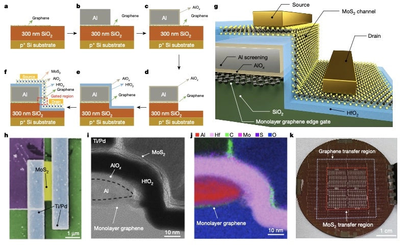
- Uses graphene edges as gate electrodes.
- Controls a vertical MoS2 channel.
- Gate length: 0.34 nm (ultra-small).
- Enables smaller, faster, energy-efficient electronics.
- Promising for next-gen compact devices.
Reference Article -- Vertical MoS2 transistors with sub-1-nm gate lengths
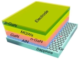
- Supports GaN and other materials' epitaxial growth.
- Reduces lattice mismatch and thermal stress.
- Enhances material quality and device performance.
- Enables thinner, more efficient structures.
- Promotes development of LEDs, power electronics, and RF devices.
- Facilitates scalable, high-quality production.
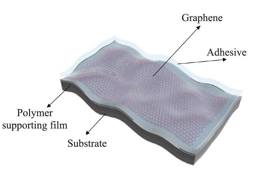
- Acts as water and oxygen barrier.
- Protects sensitive materials from moisture and oxidation.
- Enhances durability of electronics, food packaging, and pharmaceuticals.
- Ultra-thin, lightweight, and flexible.
- Suitable for flexible displays, solar cells, and medical devices.
- Promotes longer product shelf life and performance stability.
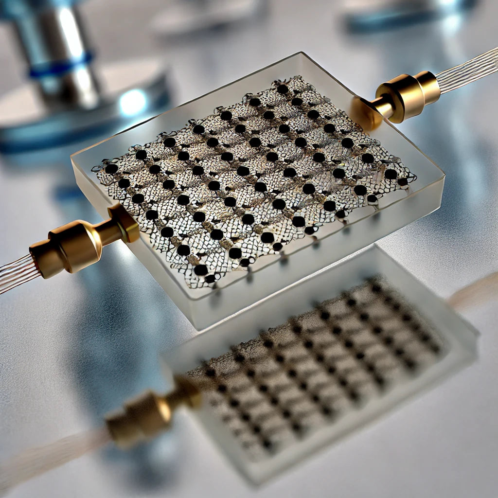
- Enables highly sensitive detection of gases, chemicals, and biomolecules.
- Fast response time and low detection limits.
- Flexible and lightweight for wearable and implantable devices.
- Used in environmental monitoring, healthcare, and industrial safety.
- Supports real-time data collection and IoT integration.
- Promotes development of next-gen medical diagnostics and smart sensors.
More Possibilities
In addition to the relatively clear application scenarios mentioned above, researchers from universities and research institutes around the world have also purchased graphene film wafers from us and utilized our transfer services. The following table outlines the target substrates and application areas corresponding to our transfer services.
Devices
Gallium nitride epitaxy
Remote epitaxy on nitride
Metasurface radar countermeasures, time-modulated reflectors
Preparation, characterization, and property measurement/regulation of 2D materials
Ultra-small node carbon-based devices and processing methodologies
Gallium nitride epitaxy
Transport mechanisms of molecular crystal materials and applications in high-performance optoelectronic devices and circuits
