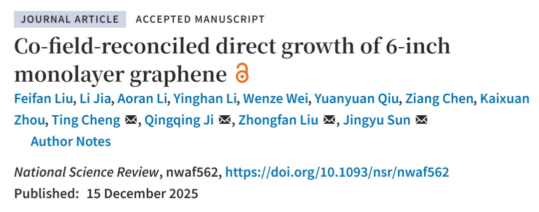
A collaborative research team led by Professor Jingyu Sun from Soochow University, Academician Zhongfan Liu from Peking University and the Beijing Graphene Institute (BGI), and Researcher Qingqing Ji from ShanghaiTech University, has published a research article in National Science Review entitled “Co-field-reconciled direct growth of 6-inch monolayer graphene.”
This work presents a scalable strategy for the direct wafer-scale growth of high-quality monolayer graphene on insulating substrates, addressing a long-standing challenge in graphene manufacturing and integration.
——————————————————————————————
Background
Graphene has attracted extensive interest in electronic and optoelectronic devices owing to its exceptional electrical, optical, and mechanical properties. However, achieving wafer-scale synthesis of high-quality graphene, particularly on insulating substrates, remains highly challenging.
Conventional chemical vapor deposition (CVD) methods typically rely on metal catalysts and require subsequent transfer processes. These transfer steps often introduce contamination, defects, and non-uniformity, which significantly degrade film quality and device reliability. As a result, direct growth of graphene on target insulating substrates has emerged as a promising alternative for next-generation graphene-based device integration.

Figure 1. Direct growth of monolayer graphene on a 6-inch sapphire wafer.
——————————————————————————————
Co-Field-Reconciled Growth Strategy
In this study, the research team proposed a co-field-reconciled growth strategy, in which both the thermal field and gas flow field are precisely regulated to enable the direct growth of monolayer graphene on 6-inch sapphire wafers.
By introducing graphite spacers to homogenize the substrate surface temperature and optimizing the gas distribution (showerhead) design to improve flow uniformity, the researchers significantly enhanced growth uniformity and batch-to-batch reproducibility. This synergistic control of temperature and flow fields ensures stable growth conditions across the entire wafer.

Figure 2. Thermal-field and gas-flow-field regulation enabling uniform graphene growth on a 6-inch sapphire wafer.
——————————————————————————————
Experimental Approach and Mechanism Insights
The experiments were conducted in a home-built cold-wall CVD system, featuring an efficient carrier self-heating mode enabled by electromagnetic induction heating of a graphite susceptor.
Key experimental conditions included:
Annealing of 6-inch sapphire wafers at 1400 °C for 10 minutes
Graphene growth under an Ar/H₂ atmosphere at 3000 Pa, with methane (CH₄) introduced as the carbon source
Comprehensive characterization was performed using Raman spectroscopy, transmission electron microscopy (TEM), atomic force microscopy (AFM), and four-probe electrical measurements.

Figure 3. Structural and spectroscopic characterization of the as-grown monolayer graphene on a sapphire wafer.
In parallel, theoretical calculations and ab initio molecular dynamics (AIMD) simulations revealed that the cold-wall CVD environment significantly reduces the energy barrier for methane decomposition, accelerates reaction kinetics, and effectively suppresses multilayer nucleation, thereby favoring uniform monolayer graphene formation.

Figure 4. Theoretical investigation of monolayer graphene formation based on ab initio molecular dynamics (AIMD) simulations.
——————————————————————————————
Wafer-Scale Performance and Device Demonstration
The directly grown graphene films exhibit:
Excellent crystal quality
High spatial uniformity across the 6-inch wafer
Consistent electrical performance
To validate device-level uniformity, the team fabricated 6-inch wafer-scale top-gated graphene field-effect transistor (GFET) arrays. The devices demonstrated highly consistent electrical characteristics, with average room-temperature carrier mobility comparable to state-of-the-art graphene technologies, confirming the scalability and reliability of the proposed growth method.

Figure 5. Electrical properties of the 6-inch wafer-scale graphene film.
——————————————————————————————
Key Innovations
* Co-field-reconciled growth strategy integrating thermal-field and flow-field regulation to improve uniformity and reproducibility
* Direct growth of high-quality monolayer graphene on 6-inch sapphire wafers, eliminating the need for transfer
* Mechanistic insights into reduced methane decomposition barriers and suppressed multilayer nucleation in cold-wall CVD systems
* Wafer-scale GFET arrays with uniform device performance and competitive room-temperature mobility
* Substrate versatility, with demonstrated applicability to other insulating substrates such as SiC, WC, Si₃N₄, and SiO₂
——————————————————————————————
Conclusion and Outlook
This work demonstrates a robust and scalable route for the direct wafer-scale growth of monolayer graphene on insulating substrates through synergistic regulation of thermal and flow fields. The proposed strategy significantly improves growth uniformity and batch reproducibility, while enabling high-performance graphene device integration without transfer-related drawbacks.
The results highlight the strong potential of this approach for large-scale integration of two-dimensional materials, paving the way for future advances in nanoelectronics, optoelectronics, and wafer-level graphene manufacturing.
——————————————————————————————
Journal: National Science Review
Title: Co-field-reconciled direct growth of 6-inch monolayer graphene
DOI: https://doi.org/10.1093/nsr/nwaf562


Leave a comment
All comments are moderated before being published.
This site is protected by hCaptcha and the hCaptcha Privacy Policy and Terms of Service apply.