Background
Heteroepitaxy is a cornerstone of modern semiconductor technology. Its success relies heavily on high-quality epitaxial layer growth on single-crystal substrates with matched lattice structures and surface symmetry. Among these, ultra-flat single-crystal Cu(111) surfaces have attracted significant attention as ideal platforms for growing high-quality, wrinkle-free single-crystal graphene and hexagonal boron nitride (hBN) films.
Compared to sapphire-based copper substrates prepared via precision magnetron sputtering or AGG-Cu foils (based on abnormally grown grains), Bridgman-grown, cut, and polished (BCP) single-crystal copper wafers offer superior cost-effectiveness, reliability, and surface smoothness. These advantages make them a highly promising substrate for graphene film epitaxy.
The Challenge
During high-temperature processing, BCP-Cu wafers have long suffered from a critical challenge - reserse single-crystallization. Dislocations and residual stress—introduced during cutting and polishing—tend to accumulate near wafer edges. Under subsequent high-temperature annealing, these stress-concentrated regions act as nucleation sites for abnormal recrystallization, resulting in grain boundary formation, surface roughness, and loss of single-crystal integrity.
This phenomenon has prevented BCP-Cu wafers from being compatible with standard high-temperature graphene growth protocols, leaving the technology largely unexplored in academia for over a decade.
The Breakthrough
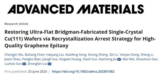
On June 25, 2025, a research team led by Academician Zhongfan Liu, along with Dr. Luzhao Sun and Dr. Kaicheng Jia of Peking University and the Beijing Graphene Institute, introduced a novel annealing strategy to suppress abnormal recrystallization.
This method successfully overcame the reverse recrystallization problem of BCP-Cu(111) wafers at high temperatures, achieving 96.6% single-crystallinity and 0.81 nm surface flatness on 2-inch copper wafers—providing an ideal substrate for graphene epitaxy.
Experimental Results
Compared to AGG-Cu(111) foils with rough surfaces, graphene grown on BCP-Cu wafers exhibited:
97.13% domain orientation consistency
Zero multilayer growth
Significantly reduced wrinkly density after transfer
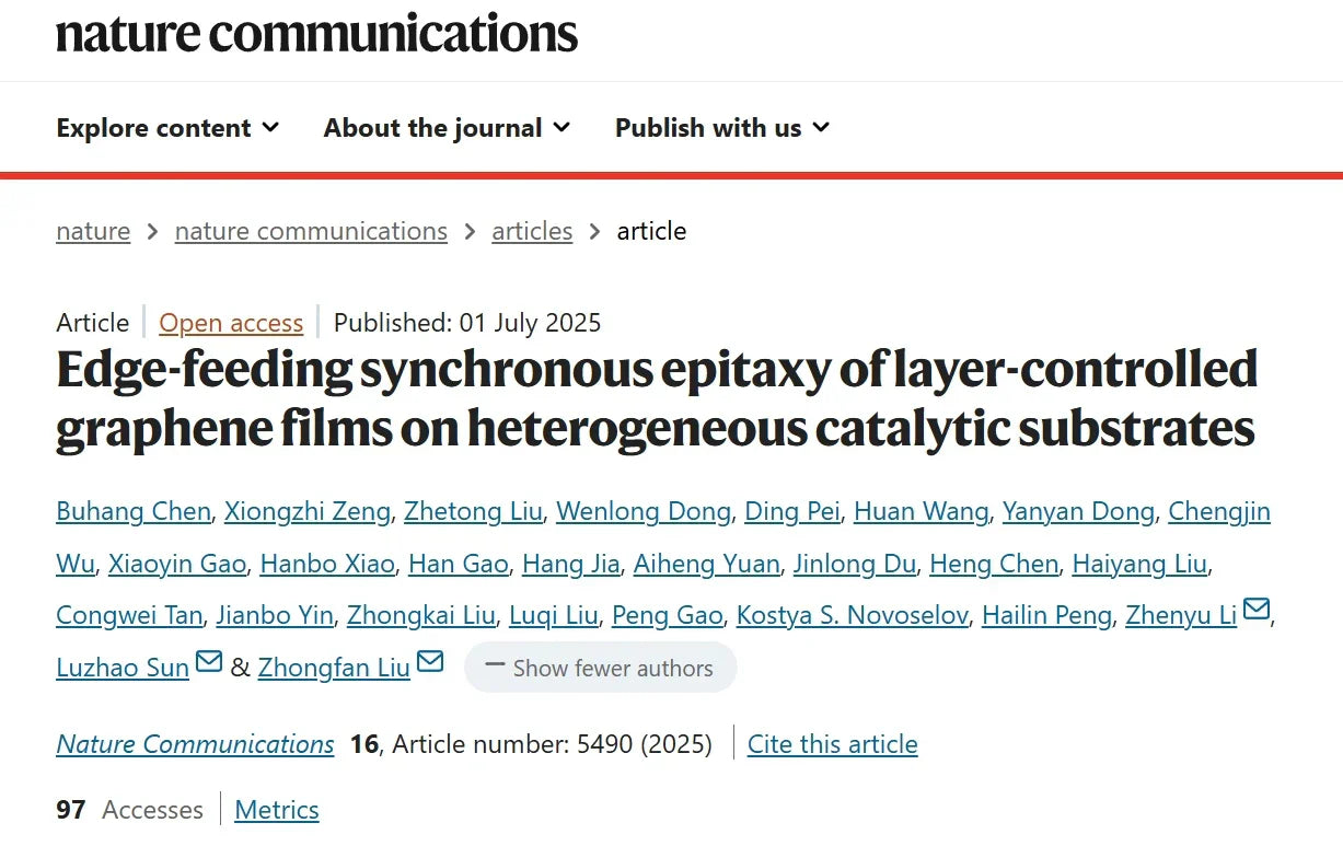
This work not only offers deep insight into 2D material heteroepitaxy, but also presents a cost-effective, scalable solution for wafer-level 2D material synthesis.
Summary and Outlook
This study introduces a novel thermal treatment method for single-crystal metals, effectively suppressing stress-induced recrystallization and maintaining both crystallinity and surface flatness. Especially applicable to cold-processed single-crystal metals (cutting, shaping, precision polishing), this customized heat treatment process ensures compatibility with high-temperature film deposition and post-processing techniques such as material compounding.
The work lays a strong technical foundation for scalable, high-quality graphene growth and offers a promising pathway for the cost-effective, wafer-scale production of 2D materials.
For more information:https://doi.org/10.1002/adma.202501582


Leave a comment
All comments are moderated before being published.
This site is protected by hCaptcha and the hCaptcha Privacy Policy and Terms of Service apply.