

Recently, Beijing Graphene Institute Co., Ltd. (BGI) signed a long-term strategic cooperation agreement with a research group from Tsinghua University. According to the agreement, BGI will provide high-quality single-crystal graphene wafers and customized graphene film transfer services, which will be utilized in the manufacturing of high-end components such as sensors and chips.
In response to Tsinghua University's specific requirements for graphene films, BGI initially proposed three solutions: polycrystalline graphene film transfer, single-crystal graphene film transfer, and single-crystal wafer graphene film transfer. After sample testing, the high-quality graphene films obtained through the damage-free transfer of single-crystal graphene wafers successfully met the required standards and received high recognition from the client.
Single-Crystal Graphene Wafer Technology
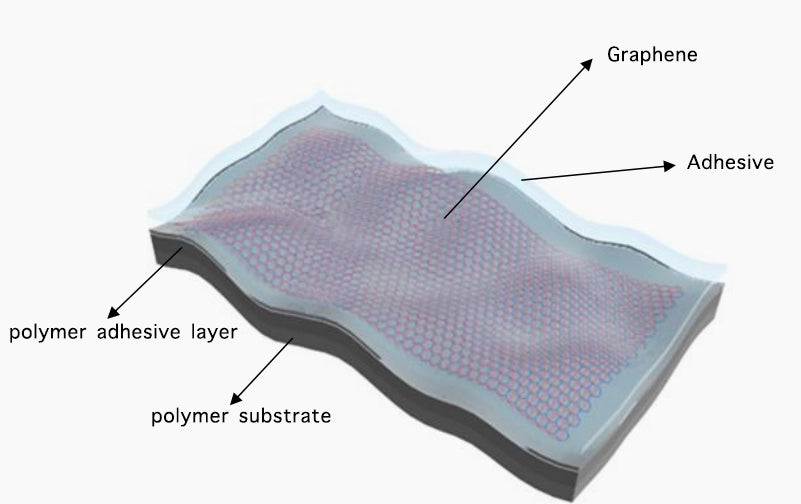
The epitaxial growth of ultra-smooth single-crystal graphene films on flat Cu(111) wafer substrates is a key method for preparing high-quality graphene films aimed at electronic device applications. By leveraging interface bonding forces and thermal stress engineering, single-crystal graphene wafers eliminate wrinkles and terrace constraints, reducing surface roughness to below 1nm. However, these graphene films, once grown on wafers, must be transferred to target substrates such as hafnium dioxide (HfO2), silicon dioxide (SiO2), alumina (Al2O3), and zirconia (ZrO2). Traditional transfer techniques can lead to structural damage and contamination, affecting the electrical properties of the transferred graphene films.
Innovative "Dry Transfer" Method
To address these challenges, BGI has continuously provided high-quality graphene materials and transfer services. The company’s innovative transfer method enables damage-free transfer of high-quality single-crystal graphene wafers (4 and 6 inches) onto rigid substrates. This pioneering "dry transfer" method effectively prevents water and oxygen doping. The transferred graphene films maintain excellent integrity (with a completeness rate exceeding 99%) and uniformity, while polymer residues on the graphene surface are significantly reduced due to direct separation from the transfer medium.
BGI’s transfer method forms a uniform oxide layer between the graphene and the copper wafer, weakening the interaction between graphene and the growth substrate. The method also uses heating to mix different types of polymers, reducing interface stress and preventing organic solvent-induced intercalation between graphene and the target substrate, thus avoiding structural damage during the transfer process. Moreover, the entire transfer process avoids the use of strong oxidizers, acids, or bases, allowing single-wafer transfers to be completed within 15 minutes, significantly improving efficiency.

Collaborations and Future Prospects
Currently, BGI’s independently developed single-crystal graphene wafers and transfer services have established collaborations with Tsinghua University, Peking University, the Suzhou Institute of Nano-Tech and Nano-Bionics, and other academic institutions. Looking ahead, BGI is committed to advancing research in high-end graphene technologies and expanding industrial applications. Through continuous innovation, BGI aims to lead the industry, positioning graphene as a key material for the future. With relentless effort and win-win collaborations, the company seeks to unlock graphene's vast potential in multiple fields, paving the way for a new chapter in graphene technology and industry development.
Leave a comment
All comments are moderated before being published.
This site is protected by hCaptcha and the hCaptcha Privacy Policy and Terms of Service apply.