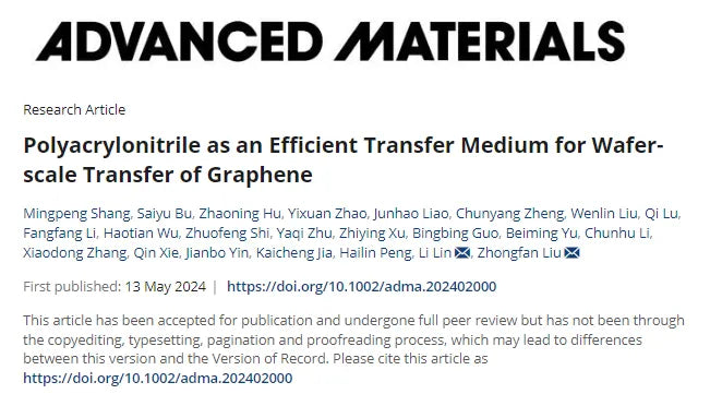
Researchers from Peking University and the Beijing Graphene Institute (BGI), led by Academician Liu Zhongfan, have discovered that polyacrylonitrile (PAN) can be used as a polymer medium for transferring wafer-scale graphene. PAN also serves as an encapsulation layer for high-performance graphene devices, eliminating the need for its removal during device fabrication. This innovation has enabled the crack-free transfer of 4-inch graphene to SiO₂/Si wafers and the successful wafer-level manufacturing of graphene-based field-effect transistor (FET) arrays, demonstrating uniform high carrier mobility (~11,000 cm²/V·s) and long-term stability at room temperature without significant doping.
Wafer-Scale Transfer and Encapsulation Using PAN
Due to the strong interaction between PAN and graphene, 4-inch graphene wafers were successfully peeled from the copper substrates and laminated onto SiO₂/Si wafers with pre-fabricated electrodes. After transfer, the PAN remains on top of the graphene, serving as an encapsulation layer for post-device fabrication. Optical microscopy confirmed over 99.0% integrity of the transferred graphene on the 4-inch SiO₂/Si wafer.
Unlike traditional methods using etching or bubble intercalation, which introduce doping due to water contact, this dry transfer process avoids such doping and improves electronic performance. The graphene was transferred and laminated in a dry state, preserving its high carrier mobility. Through photolithography, the graphene covered by PAN was patterned into Hall bar structures, allowing the fabrication of 400 devices across the wafer. The average carrier mobility reached approximately 11,000 cm²/V·s, with a peak of around 14,000 cm²/V·s, meeting the stringent requirements for graphene electronics and photonics.

Uniformity and Quality of PAN/Graphene Transfer
A key aspect of the research was ensuring that no additional doping was introduced during the encapsulation process. PAN/graphene devices exhibited a narrow 2D Raman peak full width at half maximum (FWHM) of approximately 25.1 cm⁻¹, indicating reduced doping and strain levels. This reduced doping was uniformly distributed across the entire wafer, as confirmed by large-area Raman characterization.
The Dirac point across the wafer was near zero, with an average value of approximately 0.33 V, further confirming the low and uniform doping levels. In comparison, devices using PMMA, PC, or PI for graphene transfer showed significantly lower mobilities and larger shifts in the Dirac point due to strong p-type doping.

Long-Term Stability and Easy Removal of PAN
The stability of PAN/graphene devices was also evaluated over time. After one week of air exposure, the FWHM(2D) of PAN/graphene showed minimal change, while the carrier mobility decreased only slightly, from 11,429 to 11,121 cm²/V·s. In contrast, bare graphene devices experienced a more significant reduction in mobility and a notable shift in the Dirac point due to the adsorption of moisture and impurities from the air. PAN acted as an effective barrier against water vapor and oxygen, ensuring long-term stability.
In applications where exposed graphene surfaces are required, such as in sensors and MEMS, the PAN layer can be easily removed after device fabrication. Post-removal, the graphene on the 4-inch SiO₂/Si wafers maintained over 99% integrity, and the average carrier mobility of the devices was measured at 8,579 cm²/V·s, with no visible polymer residue on the graphene.


Conclusion
This research demonstrates the use of PAN as an effective medium for the wafer-scale transfer of 2D materials like graphene, providing excellent encapsulation and preventing doping. The study successfully fabricated wafer-scale graphene devices with high carrier mobility (~11,000 cm²/V·s), near-zero Dirac points (~0 V), and outstanding uniformity and stability at room temperature. The work introduces a new concept for 2D material transfer, in which multifunctional transfer polymers like PAN can be retained to enhance device performance, providing a reliable pathway for producing high-performance, large-scale 2D material devices.
Original article: https://doi.org/10.1002/adma.202402000


Leave a comment
All comments are moderated before being published.
This site is protected by hCaptcha and the hCaptcha Privacy Policy and Terms of Service apply.